

Recent News
CHTM Joins NSF's NQVL Pilot Projects
August 9, 2024
OSE PHD, Dr. Xuefeng Li - Wins The Outstanding Interdisciplinary Graduate Programs Award
May 10, 2024
Dr. Ali Rastegari - 2024 OSE Best Dissertation Award Winner
May 10, 2024
2024 OSE Spring and Summer Graduates
May 10, 2024
News Archives
Emma Renteria’s doctoral research project seeks to solve off-the-grid electrical production
August 1, 2017 - Sharon Steely
Emma Renteria
Emma Renteria is a doctoral student working in Professor Ganesh Balakrishnan's Optoelectronics Research Group, which specializes in compound semiconductors with a focus on high power lasers, solar cells and novel nano-structures. Renteria earned her Bachelor of Science in Chemical Engineering from The University of New Mexico (UNM), and is now seeking her Ph.D. at UNM’s School of Engineering, conducting her research at UNM's Center for High Technology Materials (CHTM).
Thin-film Gallium Antimonide (GaSb) Thermophotovoltaic Cells
Renteria's doctoral research project explores the generation of electricity from heat sources besides the sun (which powers solar cells). This provides solutions for off-grid electricity production in situations which may not have reliable or very much sun exposure, such as remote locations in very northern or southern latitudes.
Her doctoral project focuses on conversion of electricity from heat in a thermophotovoltaic (TPV) cell. Conversion of electricity from local heat sources such as propane is a way for a residence or commercial enterprise to be off-the-grid while providing both warmth and electricity. Waste heat from industrial processes is another example of source heat, which is another efficiency in the use of natural resources and may contribute to sustainability on multiple levels.
TPV cells produce greater energy output than solar cells.
The proximity of the TPV cell to the radiant heat source (for example, a propane gas flame) means the TPV cell can convert many more watts of electricity than a “solar cell” of the same size. (“Solar cells” are a common term, but refer only to TPV cells which absorb the infrared spectrum of sunlight to convert into electrical energy.)
The excess heat must be removed from the TPV cell for it to function.
Because it operates in close proximity to the heat source, a TPV cell which converts radiant heat into electricity can get very hot. For example, a TPV cell may be exposed to a propane flame, which can have a temperature between 900°C and 1500°C (~ 2700° F). In addition, excess energy absorbed by the cell is converted to heat.
At temperatures greater than 80°C (176°F), the performance of a TPV cell begins to deteriorate. Therefore, TPV cells are best operated at temperatures of 80°C or less.
The ability to remove heat faster and more efficiently is critical to the use of TPV cells, as TPV cells must be cooled down to operating temperature from their exposure to the heat source.
The cells in a TPV generator are mounted on an insulating substrate that is patterned with a metal layer to connect the cells and form an array. Then, the TPV array is attached to a heat sink. Thus, the excess heat produced in the active layers of the TPV cells must travel through the Gallium Antimonide (GaSb) substrate (where the cell was grown), the insulating substrate, and the solder to the heat sink. Because these substrates have high thermal resistance, especially the growth substrate, they slow down the process of transferring heat to the heat sink.
The proposal of Renteria's doctoral research is to explore ways to eliminate the substrate and thus eliminate thermal resistance to the transfer of excess heat to the heat sink from the active layers of the TPV cell.
In her research, Renteria uses a synthetic diamond layer as an insulating substrate. The diamonds are created by chemical vapor deposition (CVD). The CVD diamond is an excellent heat spreader. It is not electrically conductive but has a very high heat conductivity so heat moves through it quickly. Mass manufacturing of the proposed TPV cells will not have to use the expensive CVD diamond, although that is used in the experimental prototypes.
Experimental procedures
Renteria is experimenting with a way to obtain a usable thin film of the active GaSb layer of a TPV cell. In her experiments, this layer is grown via the Molecular Beam Epitaxy (MBE) reactor capability available at CHTM, where a single crystal may be created by building up orderly layers of molecules on top of a substrate. Growth of the TPV cells molecule by molecule takes four to five hours depending on the thickness of the layers to be grown.
A high crystal quality GaSb cell grown on a GaSb substrate is preferred. However, the isolation of III-Sb epitaxial layers from GaSb substrates is a difficult process since the existing wet etchant solutions for Sb based materials have very low selectivity. Hence, an alternative must be considered.
In contrast to antimonide compounds, arsenide materials have a mature etch technology. Gallium Arsenide (GaAs) substrates can be removed with a variety of highly selective etchants using a high aluminium content Aluminum Gallium Arsenide (AlGaAs) etch stop layer.
Growing a GaSb active layer on a GaAs substrate is another approach. In this case, the problem is in the growth of the layers, which creates defects which will degrade the performance of the cell. However, a technique has already been developed to minimize the number of defects.
Another approach is to explore an active Indium InGaAs ayer on an Indium Phosphide (InP) substrate. This produces no defects and no problems in isolating the thin film.
The most challenging TPV cell setup which Renteria is exploring is a GaAs/GaSb active layer on a GaAs substrate, due to the challenge of removing the substrate without affecting the active layer. In this system, an additional buffer layer of GaAs is needed in between the active layer and the GaAs substrate. (See Figure 1 below.)
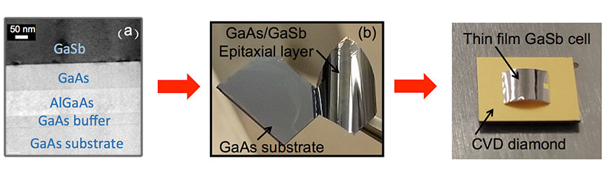
Figure 1
(a) Cross-section transmission electron microscopy (XTEM) image of a GaSb sample grown on a GaAs substrate with an AlGaAs sacrificial layer for ELO purposes
(b) Image of sample after etching the AlGaAs sacrificial layer
(c) Example of a thin film cell ready to be bonded to CVD diamond
Upon the removal of the substrate where this layer is grown, the fully processed thin film cell is then transferred to a CVD diamond. The substrate is removed by a wet-chemical etching process in the CHTM Cleanroom. The next steps in the research are characterization and testing of the devices to determine the performance of the TPV cells. Data is collected on the voltage characteristics of the generated current. The data is analyzed graphically cell-to-cell to observe the efficiencies and to see if improvements can be made.
Collaboration
Sadhvikas Addamane and Ahmad Mansoori, other members of the Optoelectronics Research Group, assist in the research by growing the TPV thin film in the MBE laboratory at CHTM. The Air Force Research Laboratory (AFRL) provides facilities for Renteria to measure quantum efficiencies and Renteria sends cells for characterization to Purdue University collaborators.
Paying it forward with mentoring
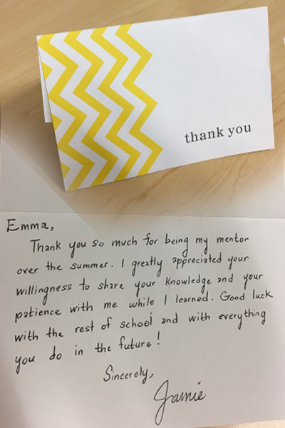
Renteria has taken on the mentorship of high school students for summer internships for several years. This summer, she supervised three interns with diverse interests — psychology, computer science and bioengineering. All three of her interns plan to continue their studies at UNM. She spends as much time as she can with the students so they can get the most out of their summer internship.
For the first week, the interns shadow Emma to become familiar with the research facility at CHTM. Then, Emma learns about their interests and works with each student to develop their own research project for the summer. She designs the research with the students and guides them in hands-on experiments in the laboratories at CHTM. The students take their project to completion, then document it as a poster presentation. The students present their posters at a QESST Conference, held at Arizona State University. Twelve universities are part of the QESST ERC (Quantum Energy and Sustainable Solar Technologies, a National Science Foundation Engineering Research Center). The conference is an exciting platform for the students, exposing them to the greater possibilities of a career in STEM (Science, Technology, Engineering, Mathematics).
The students learn hands-on skills at CHTM such as:
- How to use a microscope
- Exposure to Scanning Electron Microscopy
- How to measure current voltage so that students can perform characterization of thermophotovoltaic cells
- How to remove substrates from the cells in the Cleanroom chemically by wet etch
- Photolithography in the Cleanroom
- Metal Evaporation in the Cleanroom
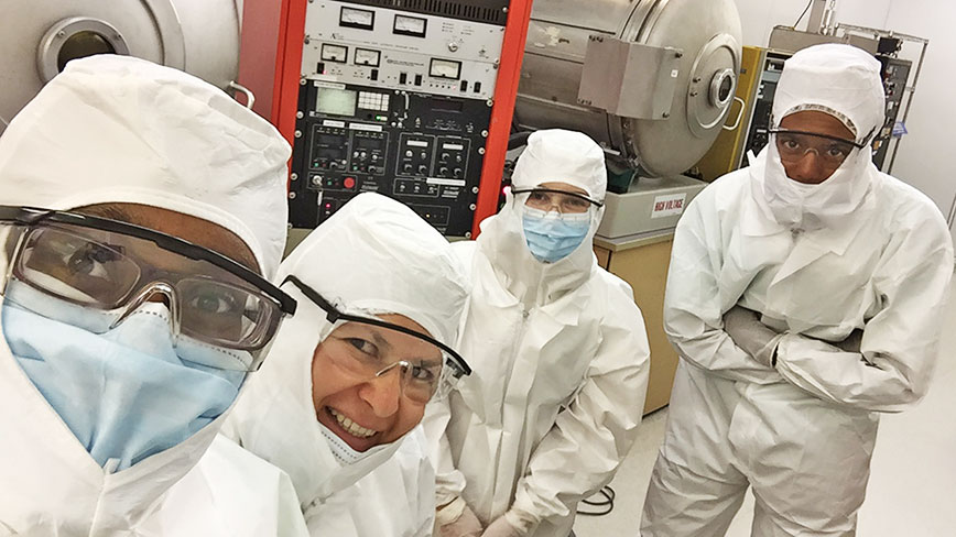
Renteria supervises each individual project for the students, and accompanies them into the Cleanroom for hands-on instruction in laboratory skills.
In addition to her high school students, Renteria has mentored four undergraduate students at UNM, some of whom have gone on to internships at Sandia National Laboratories. A student from earlier this year can now process an entire solar cell, and is ready to work in the Cleanroom on her own.
Renteria and her interns are “well-suited” for the CHTM Cleanroom
Renteria credits her own path in engineering to a couple of well-timed outreach events. In high school, Renteria joined an all-girls club, where they enjoyed a field trip to IBM. They were encouraged to consider careers that at the time were traditionally considered to be for men, such as engineering.
A luncheon titled "Focus for the Future” held at her community college in Arizona is still vivid in Renteria's memory. She sat at a table with women engineers from Intel and she was so encouraged to see that women could take their place in the engineering field, and there was a place for her too.
“That is why I am in engineering,” says Renteria. “I loved math, I liked chemistry a lot. But I didn’t really get that I could pursue these things in higher education and as a career until it was shown to me.” A booth at a career fair displayed silicon semiconductor wafers and when she held one in her hands, she connected the dots. “People in the semiconductor business are chemical engineers, electrical engineers — I could do this!”
Ganesh Balakrishnan
Renteria has been working with Professor Balakrishnan since she approached him as an undergraduate student while pursuing her Bachelor of Science degree in Chemical Engineering. She is very appreciative of Balakrishnan’s consistent positivity and guidance. While he does not have much time to spend one-on-one, he is always available for essential questions or support. As part of her participation in Balakrishnan’s Optoelectronics Research Group, Renteria has been encouraged to attend two conferences per year with the opportunity to give a talk on her work or present a poster. She is very interested in outreach opportunities and has noticed that women and minority students are sometimes amazed to meet a doctoral engineering student who speaks Spanish. She enjoys seeing the lightbulbs go off for them! It means a lot to her to show others that there is a place for them in STEM, as others had opened the door for her to discover her own field of research and discovery.