

Recent News
NQVL Design Phase Award
October 1, 2025
CHTM Joins NSF's NQVL Pilot Projects
August 9, 2024
OSE PHD, Dr. Xuefeng Li - Wins The Outstanding Interdisciplinary Graduate Programs Award
May 10, 2024
Dr. Ali Rastegari - 2024 OSE Best Dissertation Award Winner
May 10, 2024
News Archives
STC files patent application on behalf of Steven Brueck, Seung-Chang Lee for nanowire innovations
August 26, 2016 - CHTM, excerpted from STC Newsletter
Steven R. J. Brueck
Researchers at the University of New Mexico (UNM) have developed a very simple, but radically innovative approach to growing and — importantly — positioning massive arrays of nanowires. Distinguished Professor Emeritus Dr. Steven Brueck and Research Associate Professor Seung-Chang Lee with the UNM Department of Electrical & Computer Engineering and the Center for High Technology Materials (CHTM) have developed a method for catalyst-free epitaxy of single material semiconductor nanowire (NWs) or vapor-liquid-solid (VLS) epitaxy for complementary dual-material NWs with two different metal catalysts specially separated on predetermined local (111) facets for single-direction growth on a silicon (Si) (001) substrate.
VLS nanowire typically grow perpendicular to their substrates, which makes organizing and contracting them into circuits difficult and complex. Epitaxy refers to the process of depositing a crystalline layer, or film, on a crystalline substrate and is used to grow defect-free semiconductors and nano materials.
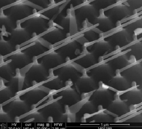
Scanning electron microscope (SEM) image of an array of InAs NWs grown on a Si(001) substrate using novel method
[The new approach] ...is an ultimate solution for NW devices because the radical innovation process reliably produces tunnel field effect transistors (TFETs) with high integration density and high current.
Additionally, no pick-up and relocation of individual NWs is necessary, which is typically required when manufacturing NW devices, and the NWs are bendable to the substrate with minimal stress and controlled manipulation.
Semiconductor nanowire (NWs) are a promising approach to future electronics as the limits to traditional scaling of silicon (Si)-integrated circuits approaches.
Electron transport in low-dimensional structures, such as nanowire, nanotubes and quantum dots, is important not only for fundamental scientific research but is increasingly relevant to future advances in electronics and photonics. These materials have extraordinary electronic, optical, thermal, mechanical and chemical properties and could be used in a wide range of nanotechnologies from biomedical to quantum-functional devices for next-generation nano electronics.
The technology has widespread applications in many areas, including use in integrated circuits (specifically transistors), semiconductors, electronic and optoelectronic devices, nano electromechanical devices, optics, and biomedical devices.
The Science & Technology Corporation at the University of New Mexico (STC.UNM or STC) has filed a patent application (reference numbers 2015-100) on the exciting new technology and is currently examining commercialization options.
Excerpted from:
• "UNM Inventors Develop Nanowires for Next-Gen Electronics," STC.UNM Newsletter, Fall 2016 Edition, Volume 32, page 2. Refer to the source article for a detailed description of the technology and process.