

Recent News
NQVL Design Phase Award
October 1, 2025
CHTM Joins NSF's NQVL Pilot Projects
August 9, 2024
OSE PHD, Dr. Xuefeng Li - Wins The Outstanding Interdisciplinary Graduate Programs Award
May 10, 2024
Dr. Ali Rastegari - 2024 OSE Best Dissertation Award Winner
May 10, 2024
News Archives
CHTM Special Seminar: Concepts for optical metrology enabled by modeling microembossing and nanoimprinting
March 20, 2017
Hayden Taylor
"Concepts for roll-to-roll inline optical metrology enabled by computationally inexpensive simulations of polymeric microembossing and nanoimprinting"
Hayden Taylor, UC Berkeley
Monday, March 27th, 10:30 a.m. - 11:30 a.m.
CHTM 101
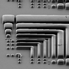
Hayden Taylor, Assistant Professor of Mechanical Engineering at the University of California at Berkeley, visits CHTM to present the discoveries of his Design for Nanomanufacturing research group in extremely fast computational techniques for simulating the imprinting and embossing of micro- and nano-scale patterns into layers of polymeric materials.
The techniques are scalable to complex geometries containing many millions of features and can be used to guide the design of processes for manufacturing microfluidics, integrated circuits, photonics, and functional surfaces.
Dr. Randall Schunk, National Laboratory Professor with the UNM Department of Chemical and Biological Engineering, said the connection to optical metrology is a rich intersection to the work that UNM conducts with the NASCENT ERC.
About Hayden Taylor:
Hayden Taylor is an Assistant Professor in the Department of Mechanical Engineering at the University of California, Berkeley. He was previously an Assistant Professor at Nanyang Technological University in Singapore, a Postdoctoral Research Fellow in the Biosystems and Micromechanics group at the Singapore-MIT Alliance for Research and Technology, and a Research Associate in the Microsystems Technology Laboratories at MIT.
He recently joined the NASCENT ERC as a faculty member.
Taylor is a member of the IEEE, the Institution of Engineering and Technology, and the Institute of Physics. He was an Institution of Electrical Engineers Jubilee Scholar 2000-4, and was a Kennedy Scholar for the academic year 2004-5.
Republished from Design for Nanomanufacturing research group
Major areas of research:
- Contact mechanics in materials processing
- Nanoimprint lithography (NIL) process modeling
- Manufacturing of polymeric microfluidic devices
- Diffractive inline optical metrology
- Materials testing for microsystems fabrication
- Optical "nanocaliper" system for thin-film metrology and rheology
- Three-dimensional holographic lithography
- Modeling of deep silicon plasma etch
Seminar abstract:
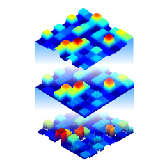
We have developed a set of extremely fast computational techniques for simulating the imprinting and embossing of micro- and nano-scale patterns into layers of polymeric materials. The techniques are scalable to complex geometries containing many millions of features and can be used to guide the design of processes for manufacturing microfluidics, integrated circuits, photonics, and functional surfaces.
The modeling approach encapsulates the polymer’s time-dependent behavior using an analytical function for its surface deformation when loaded at a single location. Meanwhile, the embossing/imprinting stamp and the substrate or web are well modeled as linear-elastic. Our approach takes a spatially discretized representation of the geometries on the stamp and finds polymer and stamp deflections in a series of iterative steps.
Republished from Design for Nanomanufacturing research group
I will describe how this modeling approach has been applied to the hot micro-embossing of relatively high-molecular-weight amorphous thermoplastics for microfluidics manufacturing. I will also describe applications in simulating nanoimprint lithography, including recent developments of the model that incorporate the spreading and coalescence of tens of thousands of picoliter-volume droplets of photocurable resin between a stamp and a substrate. I will then discuss how these mechanical process models could be used to design process-monitoring diffractive optical elements that could be incorporated unobtrusively into embossed/imprinted patterns. These process monitors would impart information to an illuminating laser beam about the performance of the embossing process, and could diagnose specific processing issues such as pressure nonuniformity, incomplete cavity filling, and demolding defects.